Dual-function devices combining CNT and ferroelectric materials
The exceptional electronic properties of carbon nanotubes provide a unique access to the physics of low-dimensional systems, and have been extensively investigated using field effect, generally with SiO2 as the gate dielectric. However, an alternative and multifunctional system can be obtained by combining carbon nanotubes with perovskite ferroelectric materials, whose switchable remanent polarization could be used to modulate the charge carrier density in an overlying nanotube. In such hybrid devices, local, significantly higher and fully reversible doping could be achieved to control the electronic properties of the carbon nanotube. Meanwhile, the carbon nanotube can act as a local electric field source for nanoscale polarization switching. The main challenge for such devices is the need for very clean interfaces between the the two materials, and their relative incompatibility for direct growth of the device structure.
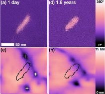
Our group is pursuing a number of alternative routes combining the two materials, including spin-deposition of short single-walled carbon nanotubes from aquaeous suspension onto patterned epitaxial Pb(Zr0.2Ti0.8)O3 thin films, and the controlled transfer of freely suspended CNT grown by chemical vapor deposition on a trenched Si-based substrate onto the target ferroelectric surface. In such devices, where we have shown repeated and reversible nanoscale polarization switching of the ferroelectric in the local field applied by the carbon nanotube, we are investigating the switching dynamics of the resulting domains, and ferroelectric field effect modulation of the carbon nanotube properties accompanying the switching, as well as the effects of carbon nanotube self-heating on the underlying ferroelectric material. In long-duration studies, we have demonstrated that the extremely small CNT-written domains nonetheless remain stable for over 18 months. We have also characterised the competing effects of charge dynamics and ferroelectric polarization on the electronic properties of semiconducting nanotubes, and explored universal conductance fluctuations in such devices at cryogenic temperatures.


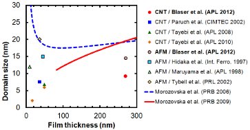
Left: (a,d) PFM phase images of a CNT-written ferroelectric nanodomain generated by a +10 V, 100 μs pulse, after a time between 1 and 600 days after switching. (e,h) Simultaneously recorded topographic images of the same areas, with the outline of the ferroelectric nanodomain. Right: Comparison of our data with previously reported domain sizes and models.

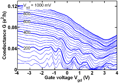
Conductance of a device containing metallic CNT on a STO sample at 4.2 K as a function of Vgd gate voltage for varying Vsd bias.